The Basics of BGA Package: An Introduction
Are you familiar with the term BGA package? If not, don’t worry! In today’s fast-paced technological world, understanding electronic packaging is essential. BGA or ball grid array packaging is a crucial component used in electronics for interconnectivity and efficient functioning of devices. This blog post serves as an introduction to the basics of bga package, their advantages over other packages, and how they are manufactured. So sit back, relax and let’s dive into the world of BGA packaging!
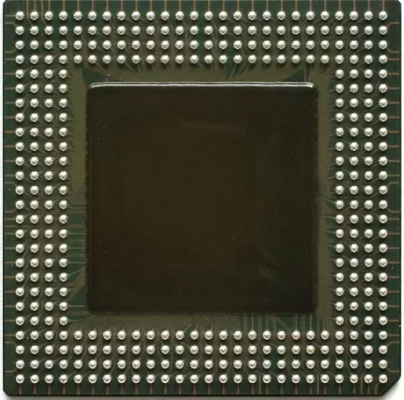
What is BGA Package?
BGA, or Ball Grid Array, is a type of surface-mount packaging used for integrated circuits. BGA packages have an array of solder balls on the underside of the package that act as connections to the Printed Circuit Board (PCB). These solder balls are typically made of lead-tin alloy and are reflowed during assembly to create a permanent connection between the IC and the PCB.
BGAs offer several advantages over other types of SMT packaging, including reduced package size, improved electrical performance, and the ability to be mounted on both sides of a PCB. However, BGAs can be more difficult to assemble than other types of packages due to the tiny solder balls and the need for special equipment and expertise.
Advantages of a BGA Package
A BGA package has several advantages over other types of IC packages:
1. A BGA package can have a smaller footprint than other types of packages, which means it takes up less space on a PCB. This is important for miniaturization of electronic devices.
2. BGAs can be more reliable than other types of packages because the solder balls make good electrical contact with the pads on the PCB. This eliminates potential problems caused by poor contact between an IC and a PCB trace.
3. BGAs can dissipate heat more effectively than other types of packages because the large number of solder balls provides a larger surface area for heat to be transferred from the IC to the PCB. This is important for preventing overheating and damage to sensitive electronic components.
Different Types of BGA Packages
Different types of bga package are available in the market, each having its own set of advantages and disadvantages. The most common types of BGA packages are as follows:
1. Flip Chip Ball Grid Array (FCBGA): This type of BGA package has the chips flipped over so that the solder balls are on the underside. This facilitates easy soldering of the chips onto the PCB. However, due to the exposed nature of the solder balls, FCBGAs are more susceptible to mechanical damage.
2. Wire-Bonded Ball Grid Array (WBBGA): In this type of BGA package, the chips are wire-bonded to the PCB. This results in a stronger connection between the chip and PCB, making WBBGAs more resistant to mechanical damage. However, due to the complex manufacturing process, WBBGAs are typically more expensive than FCBGAs.
3. Ceramic Ball Grid Array (CBGA): CBGAs feature a ceramic substrate instead of a traditional plastic one. This makes them more thermally stable and resistant to thermal shock. However, due to their fragile nature, CBGAs are more difficult to work with and are typically only used in high-end applications.
Design and Layout Considerations for a BGA Package
BGA packages are designed to provide reliable electrical and mechanical connections between a device and a printed circuit board (PCB). There are many factors to consider when designing a BGA package, including the size and shape of the device, the number of I/O pins, the pitch of the pins, the size of the PCB, and the routing requirements.
The first step in designing a BGA package is to determine the maximum dimensions of the device. The length and width of the device are typically constrained by the size of the PCB. The height of the device is determined by the number of I/O pins and the pitch of the pins.
Once the maximum dimensions of the device have been determined, it is important to consider how the device will be mounted to the PCB. There are three common methods for mounting BGA packages: solder balls, sockets, and adhesive. Solder balls are typically used for devices with pitches greater than 0.5 mm. Sockets are used for smaller pitches or for devices that require frequent replacement or testing. Adhesive is used for special applications where other methods are not suitable.
The next step in designing a BGA package is to determine the pinout. The pinout must be compatible with both the device and the PCB layout. In most cases, it is best to use a standard pinout that is widely available. However, custom pinouts can be used if necessary.
After determining the pinout, it is important
Installation Methods for a BGA Package
There are three primary methods for installing a BGA package: solder paste, thermal transfer, and eutectic bonding.
Solder paste is the most common method for installing a BGA package. This method uses a stencil to apply solder paste to the PCB. The BGA device is then placed on the board and heated to reflow the solder.
Thermal transfer is another common method for installing a BGA package. This method uses a conductive adhesive material to attach the BGA device to the PCB. The device is then heated to melt the adhesive and create a connection between the two surfaces.
Eutectic bonding is a less common method for installing a BGA package. This method uses an alloy with a low melting point to create a connection between the BGA device and the PCB. The device is heated until the alloy melts, creating a strong bond between the two surfaces.